


Toyota Grows 70mm-Thick SiC Crystal with Over 80% Yield, Paving New Path for Substrate Cost Reduction
Recently, Toyota Central R&D Labs announced in a paper titled "Modification of PVT Growth Equipment for Increasing SiC Crystal Thickness" the successful growth of a 6-inch SiC crystal with approximately 70mm thickness, achieving a nominal yield of 80.9%. This breakthrough offers a new technical approach to addressing the persistent industry challenge of high SiC substrate costs.
It is widely recognized within the industry that increasing SiC crystal thickness and growth yield is crucial for reducing substrate costs. Although the Physical Vapor Transport (PVT) technique has been developed for decades, the thickness of commercial SiC crystals has remained stagnant at 20–30mm, with limited progress over the past twenty years, constituting a major cost bottleneck hindering the widespread adoption of SiC devices. Beyond relatively low growth rates, the utilization efficiency of SiC source powder being less than 50% is also a significant factor limiting crystal thickness enhancement.
To break through this bottleneck, the Toyota team focused on structural modifications to the PVT growth furnace. The mainstream furnace technologies currently include inductive heating and resistive heating types: the former offers a simpler system structure, lower investment cost, high heating efficiency, and minimal maintenance; the latter, while enabling more precise temperature field control, suffers from higher system complexity, greater equipment cost, and heater degradation due to graphite sublimation and plasma erosion, leading to increased operational costs.
Toyota's research identified that inductive furnaces, despite their practicality, are prone to a "thermal-electrical runaway" phenomenon—where hot spots form on the sidewall of the source powder graphite crucible, creating unintended temperature gradients in the powder zone. This subsequently leads to the formation of coarse polycrystalline structures at the top of the powder zone or the bottom of the crucible, reducing powder utilization efficiency and limiting crystal thickness. Therefore, suppressing these hot spots and achieving temperature uniformity became the key to retaining the advantages of inductive furnains while enhancing crystal performance.
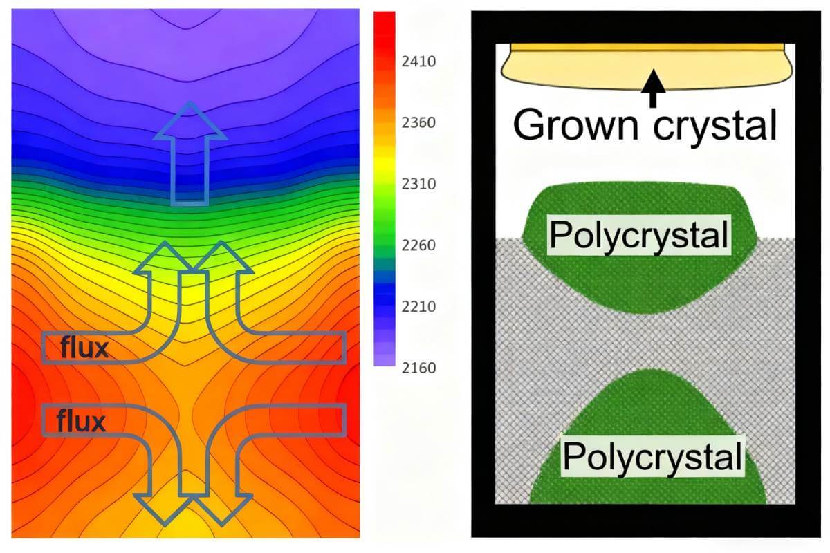
Based on this, without altering the main furnace structure or introducing expensive components, the Toyota team achieved uniform temperature control in the powder zone through innovative modifications to the graphite crucible and insulation structure. Key technical improvements include:
· Introduction of a Thermal Equalization Insulator (TEI): Replacing parts of the conventional insulation (molded graphite felt) with a stack of multiple expanded graphite sheets (e.g., GRAFOIL®, PERMA-FOIL®). This material exhibits excellent in-plane thermal conductivity (~200 W/m·K) and moderate through-thickness conductivity (~5 W/m·K), providing both thermal insulation and lateral heat spreading capability.
· Addition of a Graphite Spacer: Inserting a cylindrical graphite spacer at the bottom of the graphite crucible. The radiative heat transfer within the enclosed gap formed helps flatten the temperature distribution along the sidewall.
· Optimization of the Thermal Field Structure: Reducing the graphite thickness in the seed crystal area lowers the temperature in this region, thereby minimizing crystal defects.
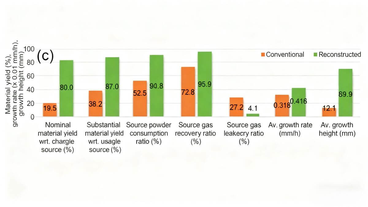
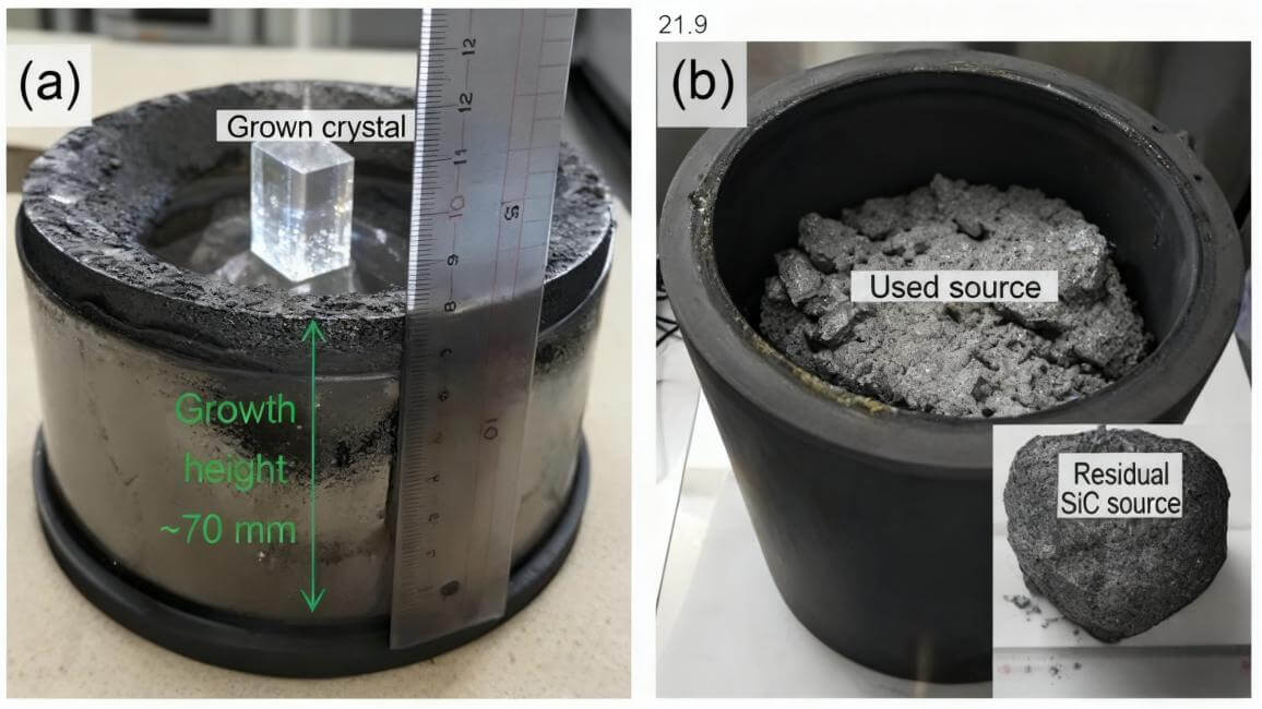
In the experimental phase, the team used a 3.5° off-axis 6-inch 4H-SiC (0001) seed crystal, along with either 3.5 kg or 4.8 kg of SiC source powder. Combined with parameter optimizations including gas leak suppression, slight crucible adjustments, and extended growth time, they successfully grew a 6-inch SiC ingot measuring approximately 69.9 mm in thickness. Experimental data showed a nominal yield of 80.9%, an actual production yield of 87.0%, a source powder consumption rate of 90.8%, and a gas leakage rate controlled at a low level of 4.1%.
Notably, despite the extended growth cycle, the average growth rate remained relatively high at 0.416 mm/h. Toyota emphasized that this result was achieved using a low-cost inductive PVT furnace combined with thermal field structure optimizations, without relying on complex or high-cost systems.
Regarding the thermal field material design, the team also disclosed key details: the crucible used was made of isotropic graphite (Ø190 mm × 320 mm); the TEI insulation layers were fabricated by stacking and bonding 0.5 mm or 1.0 mm thick expanded graphite sheets followed by baking at ~1070 K in an inert atmosphere; the bottom graphite spacer dimensions were Ø190 mm (outer diameter) × Ø160 mm (inner diameter) × 37 mm (height).
This research outcome not only demonstrates the potential of inductive PVT furnaces for enhancing SiC crystal thickness and yield but also provides a new process pathway for cost reduction, efficiency improvement, and scaled development within the global silicon carbide industry chain.