


China makes homegrown breakthrough in laser stealth dicing technology for six-inch silicon carbide ingots.
Recently, the "Research and Development of Laser Stealth Dicing Technology for Six-Inch Silicon Carbide Ingots" project, jointly undertaken by Jiangsu Third Generation Semiconductor Research Institute Co., Ltd. and the China National Innovation Center for Third Generation Semiconductors (Suzhou), has achieved a major breakthrough. The project is a key supported achievement of the Jiangsu JITRI Fellow Program, with its core technical indicators reaching the industry's advanced level, providing strong support for the autonomous and controllable development of China's silicon carbide industry.
The Jiangsu JITRI Fellow Program was initiated and implemented by the Jiangsu Industrial Technology Research Institute (JITRI), aiming to pool high-quality innovation resources and tackle critical core technologies. To date, the program has launched over 100 high-level R&D projects, becoming a major force driving industrial technology upgrading. The breakthrough project presented here is precisely one of the key achievements supported by this program.
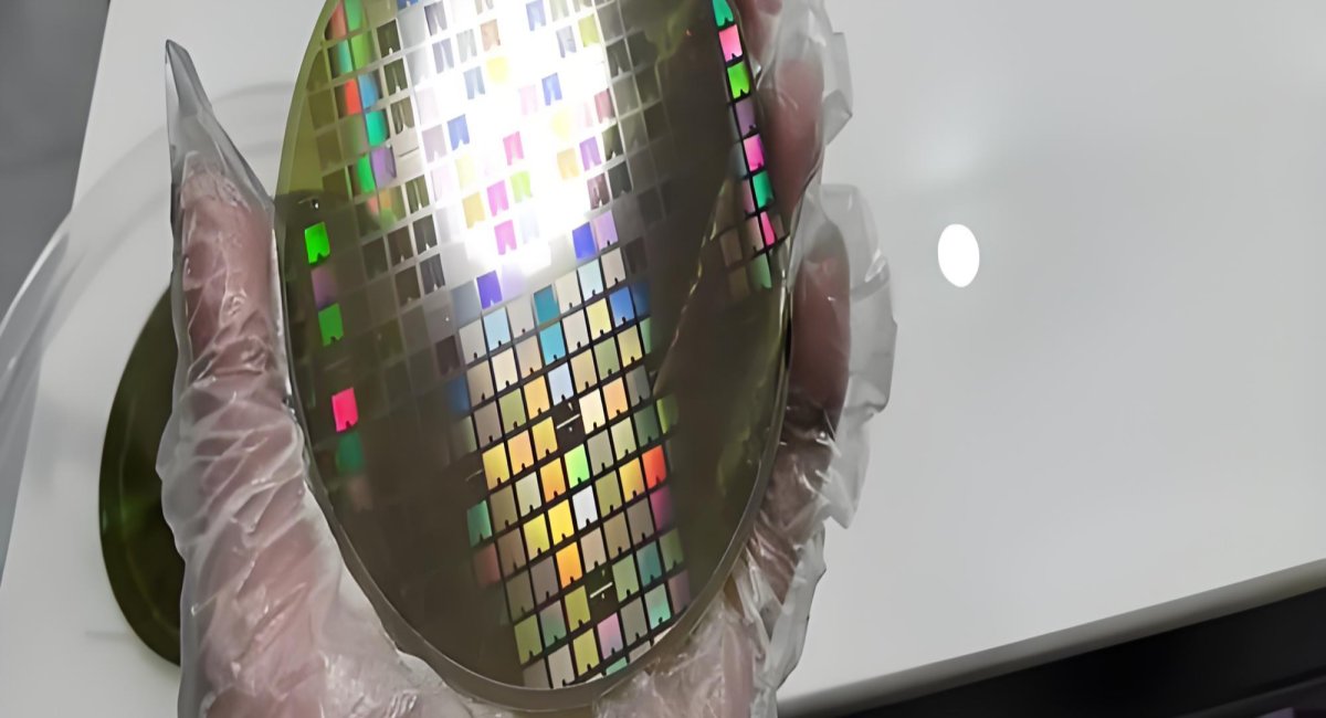
The laser stealth dicing technology that has now achieved a breakthrough delivers comprehensive improvements across multiple core performance metrics. Silicon carbide (SiC), as a core material of third-generation semiconductors, features high hardness and high brittleness, with ingot dicing having long been a bottleneck restricting industrial development. Conventional dicing processes suffer from low efficiency, high material loss, and insufficient yield, which have severely impacted the industrialization of SiC substrates and downstream devices.
Compared with conventional wire dicing, laser stealth dicing significantly shortens the single-wafer dicing time, substantially reduces ingot material loss, and steadily improves dicing yield, with overall performance far exceeding the industry average. According to the project undertaking unit, the technology has achieved key breakthroughs in dicing efficiency, yield, damage control, and thinning precision, effectively overcoming the drawbacks of conventional processes.
The China National Innovation Center for Third Generation Semiconductors (Suzhou), as one of the core undertaking entities of the project, has long focused on tackling critical common key technologies in the third-generation semiconductor field, and has established an industry-university-research collaborative and open-sharing innovation platform. To date, it has gathered diverse innovation resources, served over 500 enterprises and research institutions, and successfully resolved multiple "bottleneck" technologies. Leveraging its own R&D advantages, Jiangsu Third Generation Semiconductor Research Institute Co., Ltd. works in synergy with the Innovation Center to accelerate technology development and outcome commercialization.
This technological breakthrough fills the technical gap in the field of laser stealth dicing for six-inch silicon carbide ingots in China, breaking foreign monopoly, significantly reducing substrate production costs, and enhancing the core competitiveness of the industry. This technology also provides critical support for the domestic production of semiconductor devices used in new energy vehicles, smart grids, and 5G communications, helping China's third-generation semiconductor industry achieve high-quality and leapfrog development.